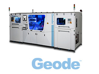
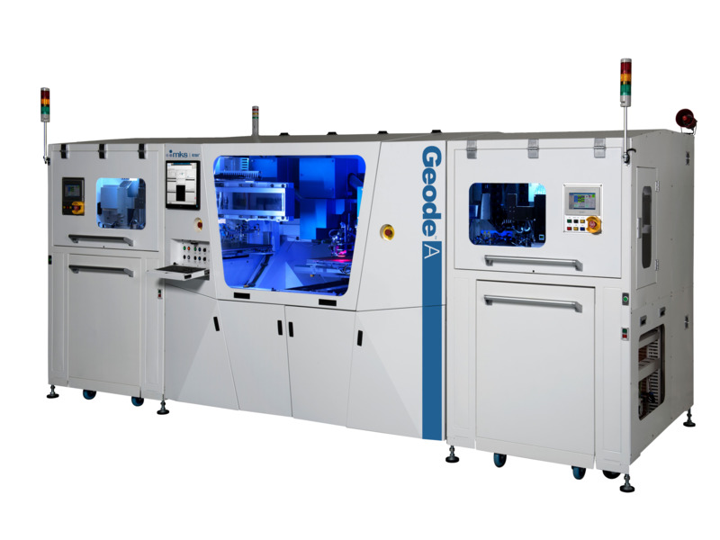
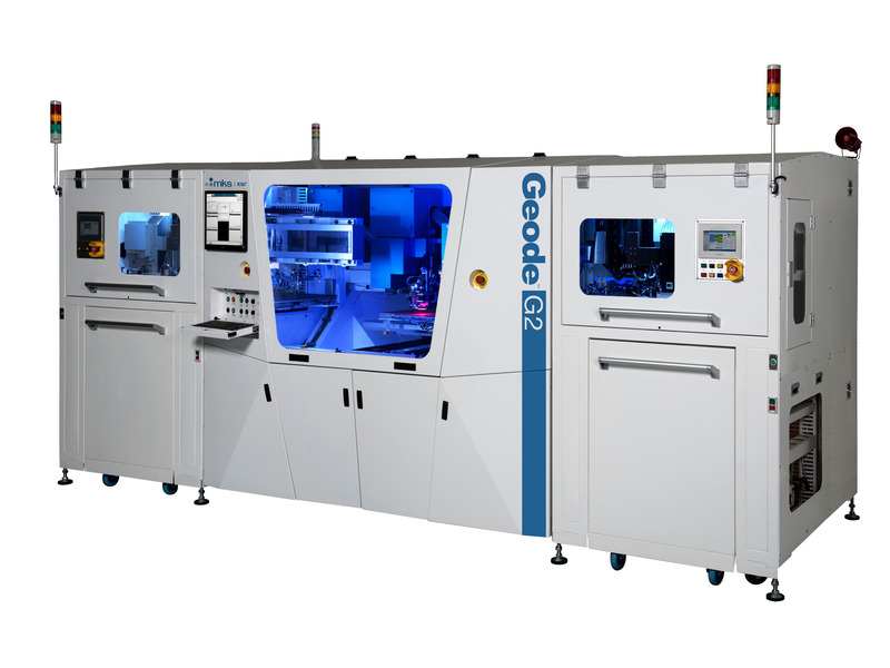
CO2 via drilling for HDI PCB manufacturing and integrated circuit packaging.
- High precision and high-speed HDI PCB & IC package manufacturing
- AcceleDrill™: Drill multiple via diameters in a single pass
- HyperSonix™: Ablate copper and material with minimal pulses See All Features
Specifications
- Average Power>300 W @ 6.5 kHz
- Peak Power2.5 kW
- Panel ProcessingDual-head two panel system
- Panel Size Range16x20 in. to 22x24 in.
- Panel Height DetectionTouchdown sensor (calibrated to align with camera focus)
- Part Thickness Range40 to 2000 um
- Energy MonitoringReal time pulse energy monitoring (programmable alarm settings)
- Automation Accuracy500 um (panel to chuck)
- ProcessingCDD/Large Window/Conformal Mask/LTH
- Scan Area20x20mm (ESI’s patented Third DynamicsTM beam positioning technology)
- Scan Frequency(per head): 5200 points per second (500 um pitch)
- ThroughputUp to 9500 pps
- Automation Panel Autoloaderstd, NG panel, Flipping
- Total System Accuracy+/- 8 um mean +3Σ
- Via Diameter Range35-200 um
- Laser Pulse FrequencyUp to 6.5 kHz
Features
Step up to new levels of precision when drilling blind and through-hole vias in a broad range of PCB and ICP materials.
Innovative CO2 laser technology, new control capabilities and applied expertise gained through decades of engineering leadership in flex, combine to deliver breakthrough levels of accuracy, throughput and yield.
Geode CO2 Via Drilling System in Action
Take a look at the latest innovations for HDI PCB Manufacturing and Integrated Circuit Packaging. Discover how the Geode can help you innovate and stay ahead.
AcceleDrill™ Spatial Distribution in Action
Outpace your competition by increasing your Rigid PCB throughput by drilling multiple via diameters in a single pass. Geode™ will enable you to process an extensive dynamic range of via size without changing the spot size.
HyperSonix™ Time & Power in Action
Your traditional Rigid PCB via drilling system may need several pulses to ablate copper & material, reducing your production yield. Increase your throughput and accuracy with Geode’s pulse chopping capabilities to ablate copper and material with minimal pulses.
RTPC - Monitor & Control in Real Time
Discover how you can increase stability and via quality with the industry’s only real-time power control. Geode™ will enable you to actively manage power fluctuation to ensure higher productivity in your Rigid PCB processing.
VDC™
Accuracy - Via density compensation improves via diameter stability, accuracy and throughput.
LiteDesign™
Footprint - Compact and lightweight system architecture allows for more flexibility in system placement and use on production floor.
AeroCore™
Integrated structural air flow supports improved thermal equilibrium and simplified maintenance.
UpTime™
Easy-access design improves serviceability, decreasing maintenance and service downtime.
Processes
- PCB Manufacturing
- Integrated Circuit Packaging
- Substrate Processing
- System Level Packaging
Materials
- Glass-woven Reinforced Epoxy Resin (FR4)
- Bismaleimide-Triazine Resin (BT)
- Ajinomoto Build-Up Film® (ABF)
- Resin-Coated-Copper (RCC)
- Teflon (PTFE)
- Liquid Crystal Polymer (LCP)
- EMC
- Ceramics
- Glass
Resources
Application Notes
Rigid PCB Processing Non-Copper Clad Dielectric Material Via Drilling Laser Direct Drilling (LDD) Comformal Mask Processing
Videos
Geode C02 Via Drilling System in Action(7:16) Inside Making a Via with Geode™: AcceleDrill™ Edition(2:13) Inside Making a Via with Geode™: Hypersonix™ Edition(1:59) Inside Making a Via with Geode™: RTPC Edition(2:39) Intra-pulse Beam Steering for High Density Interconnect via Drilling(18:18) Geode™ CO2 Laser Via Drilling Solution Meeting the Challenges of New Material and PCB Designs(1:41) Laser Drilling Solution for Precision Processing of Your HDI, SLP and ICP Applications(1:41)


